


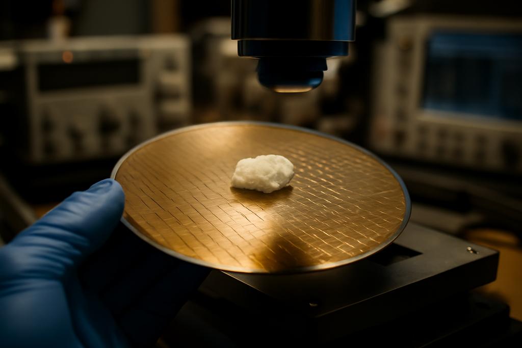
In a lab at the University of Minnesota, a new oxide is stepping into the limelight of power electronics. CaSnO3, a calcium tin oxide, sits at the edge of what researchers call ultra-wide bandgap semiconductors—materials that can tolerate enormous voltages before they fail. It’s not just about being tough; it’s about rethinking how we route electricity in devices that must stay cool while gulping high power.
Power electronics have long relied on silicon, with GaN and SiC pushing the envelope. Yet as we push voltages higher and demand reliability in harsh environments—think electric aircraft, solar inverters, and grid-scale systems—the limits of familiar materials bite back. The study from Weideng Sun, Junghyun Koo, and colleagues reports a first: a functioning metal-oxide-semiconductor field-effect transistor (MOSFET) based on CaSnO3, with performance that hints at a new path for high-voltage electronics. The work is led by Sun and Koo from the University of Minnesota, Twin Cities, with Gang Qiu as the corresponding author, and includes collaborators from Jeonbuk National University and Hongik University in Korea.
The material that makes ultra-wide bandgaps practical
CaSnO3 belongs to the perovskite family ABO3, a crystal skeleton that can host a wide range of elements while staying structurally stable. Its direct bandgap hovers around 4.7 eV, among the largest for oxide semiconductors at room temperature. That translates to a higher breakdown field—essentially a tougher barrier before the device breaks down under voltage. It is also transparent in the visible spectrum, a curious side benefit that hints at future display or sensor possibilities in rugged environments.
But bandgaps are only part of the story. In practice, turning CaSnO3 into a working transistor required coaxing electrons into the right kind of conduction without burning the material. The researchers used lanthanum doping (La) to nudge the CaSnO3 into electron-rich territory. Self-compensation, a notorious pitfall in wide-bandgap oxides, often blocks reliable n-type doping. The team’s hybrid molecular beam epitaxy growth—a skillful blend of precise atomic deposition and chemistry—delivered a 15-nm La-doped CaSnO3 film on a lattice-matched substrate (GdScO3). The result is a film that carries electrons with mobility measured in the tens of cm2 V-1 s-1 in bulk, while preserving a clean interface suited for a transistor gate. The work is a testament to the power of materials engineering when it precision-guides electronic behavior at the nanoscale.
A real MOSFET from CaSnO3 that behaves like a real transistor
To turn the material into a device, the team built a top-gated NMOS MOSFET with a carefully engineered stack. The CaSnO3 channel was thinned to roughly 11 nm and recessed to sit at the edge of depletion, while a 10-nm hafnium oxide gate dielectric sat above it, capped by Cr/Au gates. This overlapping gate geometry gives the electrostatic handshake needed to tug electrons through a wide-bandgap channel without leaking away the control signal. The structure is meticulous, and the results prove why such care matters: the transistor achieves an on/off ratio exceeding 1e8, a feat that demonstrates robust switching despite the material’s large bandgap.
When the gate is activated, the channel supports an on-state current of about 30 mA per millimeter of channel, and a field-effect mobility of 8.4 cm2 V-1 s-1. Those numbers are particularly striking for CaSnO3, where the bandgap is so wide that one might expect electron flow to be painfully sluggish. The ability to modulate the channel with a high-κ dielectric and to achieve such current with a low-resistance metal-to-semiconductor contact marks a breakthrough in turning a UWB oxide into a practical transistor. The team quantified the contact resistance using a transfer length method and found Rc to be about 0.73 kΩ·μm—one of the lowest values reported for any ultra-wide-bandgap semiconductor, a key reason the device can deliver meaningful on-state performance.
Beyond the room-temperature showcase, the CaSnO3 MOSFET demonstrates remarkable resilience. In tests up to 400 K (about 127°C), the device remains functional, though gate leakage and interfacial traps introduce some hysteresis that researchers will want to tame. The experiments also revealed a notable breakdown performance: when biased off, the device with LGD = 2 μm withstood up to 1660 V, corresponding to an off-state breakdown field of ~8.3 MV cm-1. That value sits among the highest reported for any UWB semiconductor and aligns with the theoretical limit implied by CaSnO3’s ~4.7 eV bandgap. In other words, the material’s intrinsic strength is surfacing in real devices, not just in theory.
The study’s design choices matter here. The researchers used La-doping to introduce shallow donor levels, which keeps the Schottky barrier—essentially the gate’s obstacle to electron flow—low, measured in tens of meV across the gate range. This is a crucial piece of the puzzle: without shallow donors and clean metal contacts, even a high-bandgap material would falter at the gate and fail to reach high breakdown fields. The team’s ability to quantify the Schottky barrier and to show low, temperature-stable contact resistance helps explain why the CaSnO3 MOSFET behaves so much more like a conventional transistor than a fragile oxide cousin would predict.
All of this results from a disciplined growth and fabrication pipeline. The La:CaSnO3 thin film was grown on a GdScO3 (110) substrate via hybrid MBE, then patterned into mesas, with source-drain Cr/Au contacts and a recessed channel to maximize depletion control. A 10 nm HfO2 gate dielectric, deposited by atomic layer deposition, seals the structure from leakage while still allowing strong electrostatic control. The evidence—from high-resolution X-ray diffraction to STEM-EDX mapping—paints a picture of sharp, epitaxial interfaces and uniform composition, which are essential for predictable device behavior when you’re pushing a material to its limits.
Weideng Sun and Junghyun Koo, equal contributors, and their colleagues at the University of Minnesota, with co-authors from Korea, demonstrate a rare synthesis: marrying an ultra-wide bandgap oxide with a transistor architecture that behaves like a modern device rather than a laboratory curiosity. This is a milestone that, while rooted in fundamental materials science, points toward a practical path for high-voltage, high-temperature electronics.
University of Minnesota researchers, led by Weideng Sun and Junghyun Koo, with Gang Qiu as the corresponding author, show that the CaSnO3 channel can be engineered to deliver not just resilience but real performance in a real transistor form. The collaboration with Jeonbuk National University and Hongik University in Korea underscores the international effort behind pushing perovskite oxides toward practical devices, not just intriguing materials science. The result is more than a single device; it’s a blueprint for how to turn a high-bandgap material into a versatile platform for future power electronics. The question now is how quickly researchers can translate this breakthrough into scalable manufacturing and integration with existing silicon-based systems, all while maintaining the delicate balance of doping, interfaces, and gate engineering that made this work possible.


