


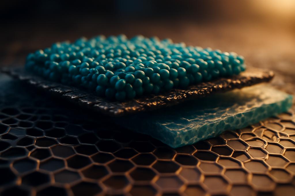
In the quiet world of electrons, tiny changes can flip the script on how matter conducts. Bilayer graphene, a pair of atom-thin carbon sheets, already behaves like a quirky musician with a distinct sense of rhythm. When you add a menagerie of molecules on top, you don’t just dampen or heighten the volume—you can rewrite the whole score of quantum interference that governs how electricity travels. A recent set of experiments takes this idea seriously: a molecular thin film of copper phthalocyanine, CuPc, sitting on bilayer graphene that’s itself perched on hexagonal boron nitride. The result is more than a tweak; it’s a controlled modulation of the very pathways electrons follow in a quantum playground.
The work, conducted by a team from California State University Long Beach, with collaborators at UCLA and Japan’s National Institute for Materials Science, is led by Claudia Ojeda-Aristizabal. The study peels back layers of complexity in mesoscopic transport—the regime where devices are small enough for quantum effects to matter, yet large enough for many electrons to dance together. It’s a space where phase coherence, chirality, and subtle scattering times don’t just matter; they shape whether electrons localize or wander freely. And CuPc is not just a passive coating: it actively reshapes the scattering landscape, nudging how bilayer graphene preserves or loses its quantum identity.
To the casual observer, a copper phthalocyanine film on graphene might look like a decorative layer, a mere ingredient in a complex stack. But in this study, CuPc behaves like a tuning dial for quantum interference. By measuring how the device conducts electricity in tiny magnetic fields at temperatures near absolute zero, the researchers decipher how often electrons keep their phase (a hallmark of quantum coherence), how readily they jump between the two valleys of bilayer graphene (the K and K’ seas of momentum space), and how the warping of graphene’s energy surface—the trigonal warping—plays with chirality, a kind of handedness in the electron’s motion. The result is a nuanced picture: the molecular film both nudges the charge balance and subtly modifies the scattering processes that underlie weak localization. This is quantum engineering at the level of a few thousand atoms across.
What makes this study stand out is not just the observation of charge transfer and modest mobility retention, but the way it connects a macroscopic transport signal—the magnetoconductance curve—to microscopic details of molecular arrangement and electronic structure. The CuPc film doesn’t simply “stick”; it forms grains with a characteristic size, arranges itself in a way that can be probed by advanced electron microscopy, and, crucially, leaves the graphene sheet with a changed, albeit still workable, quantum landscape. The team’s multi-pronged approach—transport measurements, precise back-gate tuning, and 4D scanning transmission electron microscopy to map molecular grains—reads like a detective story where every clue nudges us closer to a design principle for two-dimensional materials.
As the researchers put it in their study, the mesoscopic world is where “the quantum interference corrections to conductivity” are felt most keenly. In bilayer graphene, these corrections depend on the phase coherence, elastic scattering, intervalley scattering, and, importantly, trigonal warping. The CuPc film shifts the balance: it suppresses some warping-related scattering, inching the system back toward a regime where the carriers’ chirality reasserts itself in the localization behavior. In other words, the molecular layer becomes a lever for turning on or off aspects of graphene’s quantum personality. The discovery is exciting not just for graphene fans, but for anyone who dreams of molecular-level control over quantum transport in next-generation devices.
What weak localization reveals about graphene’s quantum choreography
Graphene’s charge carriers aren’t your ordinary electrons. In the monolayer, they behave like massless particles with a distinct “pseudospin” linked to the carbon lattice. In bilayer graphene (BLG), the situation is even richer: the carriers retain chirality, but the energy landscape folds in a way that gives the wavefunction a geometric twist as electrons wander. When electrons traverse closed loops, their quantum waves can interfere. In BLG, certain interference patterns enhance backscattering, a phenomenon known as weak localization. This quantum correction to conductivity is exquisitely sensitive to how electrons scatter elastically (how they bounce off sharp defects and atomic-scale irregularities), as well as to how long they stay phase coherent before environmental interactions scramble their quantum state. Add trigonal warping—an energy-surface deformation caused by interlayer coupling—and the plot thickens: the Fermi surface’s shape can distort interference, potentially erasing chirality’s fingerprints on localization.
Enter the CuPc molecular film. The researchers found that placing CuPc on the BLG/h-BN stack increases the weak localization signal in a telling way. From a theoretical standpoint, BLG’s magnetoconductance in a perpendicular field is described by a formula that ties the observed conductance changes to three characteristic times: the phase coherence time, the intervalley scattering time, and a combined time that encodes trigonal warping and chirality-breaking processes. By fitting their magnetoconductance data to this framework, the team could extract how these times shift with temperature and after CuPc deposition. The most striking outcome is a surprisingly long-lived coherence even after introducing molecular scatterers; the phase-breaking time declines, but only modestly, and the characteristic warping time increases, signaling a suppression of trigonal warping effects.
In practical terms, the CuPc film appears to dampen the very distortion—trigonal warping—that can blur the carriers’ chiral nature in BLG. The researchers report a two- to threefold increase in the warping-related time scale, which translates to a weaker warping influence at the energies where BLG’s peculiar band structure matters most. It’s as if the molecules are smoothing the edges of the graphene energy surface, letting the electrons wander with more of their intrinsic chirality intact when interfering paths are considered. Yet this improvement happens alongside a measurable increase in intervalley scattering, a reminder that adding molecules does not simply improve one aspect of transport; it reweaves multiple threads of the quantum fabric.
On the materials side, the team quantified a sizeable charge transfer from BLG to CuPc: about 3.6 × 10^12 carriers per square centimeter, corresponding to roughly 67 holes per CuPc grain. That electron appetite by CuPc is consistent with work function differences among the components and helps explain the observed shift of the Dirac point in gate-tuned measurements. The CuPc film acts as an electron sink, nudging the graphene into a more hole-doped regime, while leaving the mobility only modestly degraded. In fact, the mobility before deposition was 3200 cm^2/Vs and after deposition it remained robust at 2800 cm^2/Vs, a testament to the resilience of this heterostructure in the face of added molecular complexity.
All of this is anchored in careful structural characterization. The CuPc layer, deposited at room temperature and studied with a TEM-compatible control sample, shows grains averaging about 42 nanometers in size. This grain scale matters: in a graphene device, the size and distribution of molecular domains can tune how charge noise and localized scattering sites couple to electron waves as they traverse the channel. The 4D-STEM measurements—scanning TEM with a diffraction pattern captured at each scanning point—allowed the team to map grain morphology with remarkable precision while minimizing radiation damage to the delicate CuPc molecules. It’s not just clever science; it’s essential to ensure the observed transport behavior truly reflects the molecular arrangement rather than an experimental artifact.
Put differently, the CuPc film acts as a structured, uneven landscape that the electrons must traverse. The fact that mobility survived—degrading only about 13 percent—tells a story beyond abstract theory: you can coat graphene with complex organic molecules and still preserve enough of its pristine transport to learn something new about quantum interference. The nuance matters because it hints at a design principle for molecularly engineered quantum materials: you can inject donors or acceptors, you can set grain sizes, and you can tune how strongly warping fights chirality—without collapsing the device’s fundamental electronic performance.
How the experiment was built, from the trench to the molecule forest
The experimental playground starts with a clean BLG/h-BN stack, assembled with care using the Zomer method: bilayer graphene exfoliated onto h-BN, then picked up and stacked to isolate the graphene from substrate impurities. This is critical because the substrate transports a quiet soundtrack of charge puddles and impurities that can smear quantum effects. The finished device sits on a silicon gate, allowing researchers to tune the carrier density with a backgate voltage and watch how the conductance responds as electrons switch from holes to electrons with the gate sweep. The low-temperature measurements take place in a cryostat with a superconducting magnet, letting the team apply minute perpendicular fields and watch the magnetoconductance dance in real time.
CuPc was then deposited as a thin film, about 22 nanometers thick, through a carefully controlled thermal evaporation process. The deposition occurred at room temperature, while the graphene-hBN stack remained unmoved, preserving a gentle, quasi-equilibrium environment for the molecules to settle. This is a deliberate contrast to some graphene studies where molecules are solution-processed and annealed, which can introduce variability in mobility and disorder. Here, the researchers aimed for a well-controlled, room-temperature film with stable grain boundaries, so the ensuing electronic measurements could be tied back to defined molecular morphology.
Back in the transport measurements, the team observed a pronounced shift in the Dirac point after CuPc deposition, indicating hole doping of the BLG/h-BN stack. The gate voltage required to reach charge neutrality jumped by about 48 volts, a clear signature that electrons migrated from graphene to the CuPc film. Quantitatively, this translates to a transfer of 3.6 × 10^12 cm^-2 electrons, or about 67 holes per CuPc grain. The Fermi energy shifted by roughly 120 meV, consistent with a work-function difference driving electron transfer. All these numbers aren’t mere numbers; they are the fingerprints of a new equilibrium that the molecular layer imposes on the graphene’s electronic sea.
To connect the microscopic arrangement to the macroscopic signal, the team leveraged four-dimensional STEM, a technique that pairs spatial imaging with diffraction data. They found the CuPc grains in the control sample averaged 42 nanometers, a scale that fits neatly with the transport channel dimensions and explains how molecules can act as discrete scattering centers without turning the whole device into a disordered pile. The grains are large enough to support coherent scattering events within a single grain, yet small enough that electrons encounter many grain boundaries as they traverse the channel. This multi-scale picture helps explain why phase coherence survives long enough to produce measurable weak localization, even after the molecular layers are introduced.
The molecular deposition also introduced a modest increase in charged impurities in the Dirac-point region, estimated at roughly two extra impurities per CuPc grain. Yet this small impurity load does not erase the device’s quantum character. The measured elastic scattering time—how quickly momentum is scrambled by a collision—stays in the same ballpark, underscoring that CuPc, unlike some adatoms, does not catastrophically degrade graphene’s mobility. The combination of preserved mobility with altered phase coherence and warping times reveals a surprisingly gentle, tunable influence: the CuPc film is a structured perturbation, not a landslide of disorder.
The researchers’ analysis of the magnetoconductance curves goes beyond a qualitative story. By fitting the data to a bilayer graphene model that includes phase coherence, intervalley scattering, and a warping term, they extract three characteristic times: τφ, τi, and τw. The temperature dependence of τφ follows expectations—the phase coherence time shrinks as the system warms, as in most quantum-coherent systems. But CuPc’s impact is twofold: it reduces τφ more quickly with increasing temperature, indicating enhanced phase-breaking interactions, while it increases τw, extending the time scale over which trigonal warping remains a meaningful feature. In other words, the presence of CuPc moves the system toward a regime where chirality’s fingerprints on localization are more resilient.
All these insights are anchored to a single, central narrative: a molecular thin film doesn’t just sit on graphene; it participates in a dialogue with the charge carriers. The CuPc molecules are more than spectators; they act as electron acceptors, grain-forming agents, and subtle sculptors of the energy landscape. The researchers’ interpretation—that CuPc can recuperate or reinforce the carriers’ chirality in BLG’s weak localization—offers a tantalizing glimpse of how chemistry and quantum physics could intertwinedly shape the next generation of electronic materials.
Why this matters: hints for quantum materials design
The result is not a claim that CuPc is a miracle cure for graphene’s quantum quirks. It’s a demonstration that molecular-scale architecture can steer the delicate balance of quantum interference in a highly controlled way. The mobility’s modest decline alongside a coherent shift in scattering times points to a general principle: you can introduce functional molecules to a two-dimensional semiconductor without destroying its essential transport properties. This matters because the dream of quantum electronics—devices that exploit coherence and interference to perform tasks beyond classical limits—depends on precisely this kind of control.
From a wider perspective, the study speaks to a growing idea in materials science: two-dimensional heterostructures are not static stacks but adaptable ecosystems. The molecular layer can serve as a tunable dial for habitually elusive quantities like trigonal warping, which directly influences how electrons travel near the valleys of graphene’s band structure. If warping can be tamed, the pathways that preserve chirality during interference become more robust, enabling quantum devices that rely on valley or spin degrees of freedom. In the longer arc of technology, such control could impact areas from spintronics to quantum sensing, offering routes to engineer coherence times and scattering landscapes without resorting to extreme cooling or exotic substrates.
Another striking aspect is the methodological ensemble the authors assemble. They combine transport measurements with a detailed structural account—Raman fingerprinting confirms bilayer character; TEM-based 4D-STEM reveals grain sizes and crystalline order of CuPc; back-gate tuning monitors Dirac-point shifts; and magnetoconductance fits translate messy data into physically meaningful timescales. This is a blueprint for future studies: to understand quantum transport you need to know both the geography (where molecules sit and how they cluster) and the physics (how those arrangements channel or disrupt coherent electron motion). The approach underscores a practical truth: the best progress in quantum materials comes when chemistry, microscopy, and transport physics speak the same language.
The paper’s context also matters for science communication. It sits at the intersection of academic curiosity and potential technological payoff, reminding us that today’s fundamental studies can seed tomorrow’s devices. By showing that a simple, room-temperature CuPc film can modulate intricate quantum effects in BLG/h-BN, the researchers hint at a scalable paradigm for “programming” quantum materials with molecular precision. It’s not a glossy breakthrough in the sense of a new qubit, but it is a measurable, repeatable, and design-friendly advance that pushes the boundary of how we think about interfaces between molecules and quantum solids.
And although the study centers on a very specific materials stack, the underlying message travels farther: the quantum world can be gently steered by deliberate, well-characterized molecular environments. If bilayer graphene’s chiral tale can be coaxed back to reveal its hidden language of localization, then perhaps other quantum materials—topological insulators, moiré superlattices, or layered superconductors—could respond to similarly crafted molecular landscapes. The road from curiosity to application often travels through small, disciplined experiments like this one, where a molecule on a sheet of carbon becomes a lever for quantum behavior to reveal itself.
The study underscores a simple yet profound idea: in the quantum world, the line between chemistry and physics is not a chalkboard boundary but a shared playground. The CuPc/BLG/h-BN experiment shows that with careful materials design, you can sculpt how electrons interfere, how they scatter, and how long they remember their quantum state. In the hands of researchers led by Claudia Ojeda-Aristizabal at California State University Long Beach, with colleagues at UCLA and Japan’s NIMS, this line between molecular engineering and quantum transport becomes a tool, not a mystery. The implications ripple beyond graphene, inviting us to imagine a future where the choice of molecules on a 2D substrate becomes part of the design language for quantum devices.
As the team notes, the direction is not to replace silicon or to reinvent transistors overnight. It is to expand the toolbox for controlling quantum coherence in real materials, a crucial step if we want scalable, robust quantum technologies. If we ever build devices that rely on the quantum choreography of electrons, studies like these will be the footnotes that show how to tune the tempo—grains, warping, charge transfer, and all—without breaking the melody. In the end, CuPc’s quiet presence on BLG/h-BN is a reminder that sometimes the smallest collaborators yield the most surprising performances in the grand concert of quantum materials.


