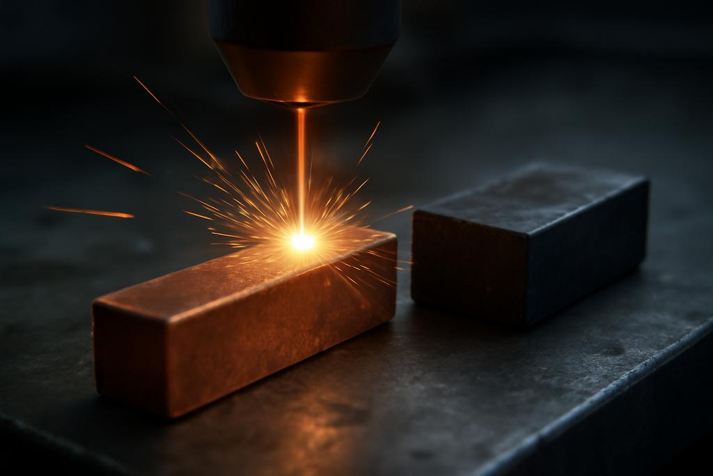
Femtosecond laser pulses are like tiny bells ringing inside a solid. The bell tolls at a tempo so fast that the electrons waltz ahead of the lattice, heating up in a flash while the atoms themselves barely move. In that瞬間, the material’s inner rules change, and so does how it responds to being poked, pressed, or carved into. A new study from the University of Stuttgart’s Institute for Functional Matter and Quantum Technologies led by Simon Kuemmel and Johannes Roth asks and answers a deceptively simple question: what if the tools we use to simulate that momentary fireworks show could themselves change with the electron temperature? The answer is a more faithful, dramatically more useful map of how copper and silicon behave under intense, ultrafast heating.
Classical molecular dynamics has long relied on fixed interaction potentials to describe how atoms tug on each other. But in the rush of a laser pulse, the electronic cloud—your electrons—gets excited and the potential energy landscape reshapes. If you want to predict what happens in the first picoseconds after the pulse—whether the surface blasts away, how a shock wave forms, or how quickly a melt front advances—you need a model that can bend with Te, the electron temperature. That’s the core idea behind an electron-temperature-dependent interaction potential (IP): a potential that morphs as the electrons get hotter. The Stuttgart team pushed this concept further by building copper and silicon IPs that track Te up to about 1.2 eV, enabling more accurate atomistic simulations of laser ablation in metals and semiconductors. The work was conducted at the University of Stuttgart, with Kuemmel and Roth steering the approach and validating it across a suite of properties against finite-temperature density functional theory (DFT) data and experiments.
A new way to simulate laser-damaged metals
The challenge is not merely to adjust a few numbers; it’s to weave a physically consistent picture across multiple layers of matter under electron excitation. The researchers build on a two-temperature model (TTM): electrons carry a distinct temperature Te, while the lattice remains at a cooler, near-equilibrium state. In laser-irradiated materials, this Te can soar to levels where the conventional, ground-state potential no longer reflects the real forces that sculpt atomic motion. The team’s strategy is to fit a copper IP that explicitly depends on Te, using a finite-temperature DFT reference landscape derived from Mermin’s formulation of density functional theory. In plain language, they’re teaching the potential to respect the fact that excited electrons change how strongly atoms bond, how stiff the lattice is, and even what the melting point might be when the pulse has barely faded.
To anchor the potential in reality, they compiled a rich set of reference data. They used three groups of configurations: affine transformations of crystal lattices to probe elastic responses, carefully deformed structures to pin down elastic constants, and non-ideal, temperature-varied structures generated from molecular dynamics at several temperatures and then fed back into static DFT calculations. All of this data—energies, stresses, forces—was then fit with a polynomial in Te to yield a continuous, Te-dependent family of potentials. The result is not a single number but a whole surface: as Te climbs, the potential morphs in a controlled, physically meaningful way, maintaining consistency with the free-energy curves and lattice dynamics that DFT tells us to expect.
The particular copper potential is built on a robust embedding energy framework—the classic EAM (embedded-atom method) form refined with a Morse-like pair potential and a transfer function designed to capture Friedel oscillations in metals. The authors also show how the same philosophy can be extended to silicon, where a modified Tersoff form (fitted to the Te-dependent cohesive free energy) does the heavy lifting. This cross-material flexibility matters: the same workflow that tethered copper to Te up to 1.2 eV could, in principle, be adapted to other materials, offering a path to universal, temperature-aware atomistic simulations of laser interactions.
Copper vs silicon: two very different dances under heat
One of the paper’s most striking results is how differently copper and silicon respond when electrons soak up energy. In copper, the Te-dependent potential predicts bond strengthening as Te rises. The lattice stiffens, elastic constants creep upward, and even the phonon spectrum shifts toward higher frequencies. In other words, the material “hardens” in the sense that atomic bonds resist distortion more, at least in the short, non-thermally melted regime following irradiation. This bond-hardening also translates into higher pressures near the surface once the lattice can’t immediately expand to accommodate the energy release. The researchers show this is not a mere artifact: the calculated elastic constants, phonon frequencies, and even the melting temperature all shift in a way that mirrors the underlying physics of electron pressure and bond strength. It’s a coherent picture that matches what one would expect from first-principles theory and, crucially, from the way experiments have observed laser-induced phenomena in copper.
Silicon, by contrast, tells a different story. Under Te up to about 0.8–1.7 eV the simulations reveal a bond-softening trend that destabilizes the diamond structure. The phonon modes soften and, in the DFT reference, certain modes even go soft at high Te, signaling the onset of non-thermal melting—a regime where the lattice loses order not because of heating in the traditional sense, but because the electronic environment has changed the “rules” governing how atoms bond and move. The MD potentials reproduce this non-thermal melting tendency with striking fidelity, including the changes in phonon spectra and the predicted shifts in the melting behavior under fixed-volume conditions that mimic the immediate post-pulse moment. The contrast is a vivid reminder that electrons, not just heat, rewrite the lattice’s mood in fundamentally different ways depending on the material’s bonding character.
Behind these trends lies a simple thread: the cohesive energy landscape moves as Te climbs. The team’s calculations show that the free-energy minimum shifts to larger volumes at higher Te, a precursor to increased pressure if the lattice can’t relax quickly enough. In copper, this push toward tighter bonding with Te helps explain the observed strengthening and the ensuing pressure wave. In silicon, the shift toward destabilization under excitation helps explain why non-thermal damage can appear even before the lattice has absorbed enough energy to melt by ordinary thermal means. The fact that a single Te-aware potential can reproduce these divergent behaviors across two very different materials is a testament to the approach’s physical grounding and potential for generalization.
Why this matters for lasers, materials, and machines
Laser ablation is widely used for micromachining, thin-film processing, and nanoparticle synthesis. Yet predicting how deep a laser will ablate a material, how its surface will crater, or how a shock wave will propagate through a sample has always been a dance of approximations. Traditional simulations treat the lattice and the electrons with a fixed, ground-state bond landscape. When the laser hits, that landscape changes, and the old rules mislead you about how far the material will melt, how fast a melt front will advance, or how much material will be ejected. The electron-temperature-dependent potentials developed in this work close a critical gap: they let the simulation follow the real-time evolution of bonding as Te soars, while still being computationally tractable enough to run large-scale, long-timescale atomistic simulations that would be impractical with full DFT.
In copper, the new IP predicts stronger bonds and higher surface pressures right after irradiation, which could alter how we interpret laser-induced shock waves and the onset of ablation. In silicon, the same approach captures the mirrored, but opposite, trend: bonds stiffen in some directions and soften in others, with a clear pathway to non-thermal melting. These insights are not just academic. They provide a more faithful bridge between electronic dynamics and mechanical response, helping engineers design laser processes that minimize unwanted damage or, conversely, maximize material removal with predictable precision. The potential’s interpolation across Te, from RT to 1.2 eV, is especially valuable for modeling real-world pulses whose exact Te trajectory depends on pulse shape, duration, and the surrounding environment.
From a practical standpoint, the team’s workflow—constructing Te-dependent potentials by fitting to a broad swath of finite-temperature reference data and validating against elastic constants, phonon spectra, and melting behavior—offers a blueprint. It’s not just copper that benefits: the same methodology has already been applied to silicon, and the paper suggests it can be generalized to other materials. The payoff is a toolkit that lowers the cost of high-fidelity simulations by avoiding full-time DFT while still capturing the essential physics of electron-lattice coupling during ultrafast heating. Researchers can now explore questions that were previously out of reach: how does a copper surface really respond to a femtosecond pulse at different pulse intensities? How does a silicon wafer behave under the same pulse when the electrons are temporarily changing the rules of bonding? And crucially, how do these microseconds-long events shape macroscopic outcomes like crater depth, ablation efficiency, and material resilience?
What it hints at for the future of materials modeling
One of the paper’s understated promises is methodological flexibility. By showing that electron-temperature-dependent potentials can be constructed with careful attention to reference data and physically meaningful interpolation in Te, the authors argue that this approach should be adaptable beyond copper and silicon. The long-term goal is to build a library of Te-aware IPs for a range of technologically relevant materials, enabling researchers and engineers to simulate laser–matter interactions with both realism and speed. The authors acknowledge limits—the copper potential they developed remains focused on Te up to around 1.2 eV, and silicon behaves in ways that resist simple extrapolation at higher Te—but they also emphasize the potential to push these boundaries with richer data sets and more sophisticated fitting strategies. In other words, this work is a strong proof of concept and a practical stepping stone toward a more predictive science of laser-material interactions.
What excites me is the human angle behind this technical achievement. It’s about listening to the electrons as they hum, watching how their heat reshapes bonds and pushes matter to do unthinkable things in the wink of a laser pulse. It’s about translating a complex quantum world into a language that our simulations can use to forecast real-world outcomes. It’s also a reminder that progress in materials science often comes from patient, meticulous work—fitting a surface that changes with temperature, validating it against multiple independent signals, and then showing that the model can reproduce the right trends across several properties. The University of Stuttgart team has produced a tool that doesn’t just describe what happens in copper and silicon under an ultrafast pump, but invites us to ask deeper questions about how electrons and atoms collaborate to sculpt matter in the moment when the rules are rewritten.
Lead researchers Simon Kuemmel and Johannes Roth at the University of Stuttgart, Institute for Functional Matter and Quantum Technologies, led the development, testing, and validation of the Te-dependent copper potential and its silicon counterpart. Their work stands as a compelling example of how targeted, physically grounded modeling can transform our ability to predict, control, and exploit laser–material interactions in cutting-edge manufacturing and materials research.


