In the grand theater of solar materials, speed is not just about absorbing sunlight but about turning that energy into usable voltage before it leaks away. For decades, gallium arsenide (GaAs) has stood as a high-performance benchmark in photovoltaics, prized for its direct band gap and stellar optoelectronic quality. Yet GaAs isn’t cheap, and its performance can still suffer when the material isn’t pristine. A team of researchers led by Gideon Kassa and Zhenkun Yuan at Dartmouth College’s Thayer School of Engineering—with collaborators from Iowa State University and UC San Diego—has uncovered a surprising contender that behaves like GaAs but with a striking twist: BaCd2P2 (BCP) appears unusually tolerant of defects and impurities. The work suggests a pathway to solar absorbers that pair solid performance with more forgiving manufacturing.
What makes this story compelling is less about a new chemical formula and more about a property scientists rarely see up close in real-world synthesis: defect tolerance. In practice, tiny unseen flaws can siphon off charge carriers or pin down energy levels, quietly crimping a solar cell’s voltage and battery-life-like persistence. The BCP study, published with the backing of Dartmouth and its collaborators, shows that even when BCP is made from less-than-perfect starting materials, it can still glow with bright band-to-band luminescence, sustain long carrier lifetimes, and exhibit an implied open-circuit voltage that rivals—and in some measurements surpasses—GaAs. The researchers don’t just observe; they also explain, with first-principles calculations, why BCP resists the nonradiative traps that typically dog GaAs. In short: BCP behaves like a GaAs analogue that can shrug off the defects that would hobble other materials.
Two central threads weave through the paper. First, the team demonstrates robust optoelectronic quality in BaCd2P2 even when precursor purity is modest. Second, and perhaps more transformative, they map the deep defect landscape with quantum-level calculations and show that the dominant defect in BCP would not drain energy as aggressively as GaAs defects do. Taken together, the results argue that BaCd2P2 could offer a more fault-tolerant, potentially lower-cost route to efficient solar absorbers. The authors behind the work are Gideon Kassa, Zhenkun Yuan, Muhammad R. Hasan, Guillermo L. Esparza, David P. Fenning, Geoffroy Hautier, Kirill Kovnir, and Jifeng Liu, representing Dartmouth, Iowa State, UC San Diego, and the Ames National Laboratory. Liu serves as the corresponding author, helping to anchor the collaboration.
BCP shines as a GaAs analogue
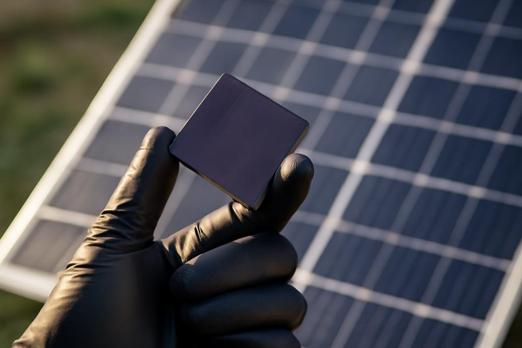
The authors began by asking a simple but powerful question: can BaCd2P2 deliver GaAs-like direct-bandgap performance while tolerating the kinds of defects that creep in during real-world synthesis? The experimental test bed was revealing. They prepared BaCd2P2 in two flavors: a powder form via solid-state reactions and a Sn-flux grown crystal. They compared the BaCd2P2 powder to well-known GaAs powders ground from 2-inch prime wafers, and they compared BaCd2P2 crystals to pristine GaAs wafers or wafers ground into powder. What they found surprised them in a very human way: BaCd2P2 produced a bright band-to-band photoluminescence peak at about 1.46 eV even when the starting materials were not pure. By contrast, GaAs powder made with the same rough synthesis showed little to no band-to-band emission at room temperature. In other words, BCP’s glow under light didn’t disappear when impurities crept into the recipe the way GaAs’s did.
The optical measurements did more than just look pretty on a spectrum. They hinted at two practical truths. First, the surface recombination velocity in BaCd2P2 can be low enough that the material maintains bright light emission despite a high surface-to-volume ratio typical of powders. Second, when BaCd2P2 was formed into a crystal, its implied open-circuit voltage under illumination remained consistently higher than that of GaAs wafers across a broad range of light intensities. If one translates implied VOC into what a cell could achieve under real sunlight, the result is a hopeful signal that BaCd2P2 can deliver strong voltages even when fabricated with manufacturing imperfections. The researchers quantified this by fitting photoluminescence spectra to a nonequilibrium emission model and extracting the quasi-Fermi level splitting, which acts like a proxy for how much voltage a material could support in a solar device. The end result: a BaCd2P2 crystal could deliver an implied VOC around 1.1 V under AM1.5-like conditions, versus about 0.95 V for GaAs under the same lens. In short: BaCd2P2 may hold its voltage where GaAs would sag under less-than-ideal conditions.
Beyond voltage, the BaCd2P2 crystal demonstrated a remarkably long carrier lifetime, an essential trait for solar absorbers. Using a combination of photoconductive current measurements and PL-based estimations, the team reported carrier lifetimes exceeding 300 nanoseconds for BaCd2P2 crystals, a value that dwarfs the roughly 5-nanosecond lifetime they measured for GaAs wafers under similar conditions. That 60-fold difference matters in devices: longer lifetimes mean charges have more time to be collected before they recombine, boosting potential efficiency. And the contrast is especially striking because these impressive lifetimes came from BaCd2P2 synthesized with relatively modest precursor purity. Taken together, the experiments knit a narrative: BaCd2P2 behaves like a GaAs cousin that doesn’t punish you for the messy parts of making it.
To complete the story, the authors turned to the bulk, to see whether what they observed at the surface and in the immediate near-surface region could survive inside the crystal. Their measurements of light-induced currents and the inferred lifetimes pointed to robust bulk behavior, consistent with a material that has less deleterious recombination in its interior. All of this built to a bold claim: BaCd2P2 could be a defect-tolerant GaAs analogue, offering a comparable energy landscape with a little more forgiveness for price-conscious manufacturing.
Why defects don’t wreck it
The second pillar of the paper is a deep dive into the microscopic reasons BaCd2P2 appears so robust. In semiconductors, defects are not just imperfections in a lab notebook—they are energetic states that can capture carriers and encourage nonradiative recombination. In GaAs, certain deep-level defects have long been notorious for draining energy away as heat rather than light, a process that damages whatever voltage a device can sustain. The question, then, is: does BaCd2P2 harbor defects that are equally, or less, troublesome?
The team turned to first-principles defect calculations, using hybrid functional density functional theory (HSE) to compute formation energies of defects across the full range of chemical potentials where BaCd2P2 and GaAs are stable. They focused on the dominant deep defects that would drive nonradiative recombination: for BaCd2P2, a cadmium antisite defect (Pc d) and its charged transitions; for GaAs, the classic EL2 defect associated with an arsenic antisite. The numbers matter because they translate directly into Shockley-Read-Hall (SRH) recombination rates: how quickly carriers get trapped and return as heat rather than contributing to photocurrent.
In BaCd2P2, the deep defect PCd’s recombination channel, across the explored chemical-potential window, yields a nonradiative rate that is substantially lower than GaAs’s EL2 channel. The calculation shows that the SRH rate in BaCd2P2 can be orders of magnitude smaller under typical photoexcitation levels. The main upshot is not just that BaCd2P2 has a lower rate in any single case, but that across the entire stability window, its deep-defect pathway remains comparatively tame. In other words, BaCd2P2 is a material in which defects are less likely to siphon off energy into the wrong channels. The authors call this a defect-resistant analogue of GaAs, one whose internal energy landscape seems kinder to carriers. And because defect physics directly constrains how close we can get to the ideal open-circuit voltage and carrier lifetimes, this result bridges theory and experiment in a way that feels unusually practical for a materials discovery paper.
One of the more technical but telling points is that the dominant deep defect in BaCd2P2, PCd, behaves differently from GaAs’s EL2 in a way that reduces nonradiative loss under the same general growth conditions. While the GaAs loss channel can span a tremendous range depending on how the material is grown, BaCd2P2 maintains a consistently lower recombination rate, which translates into brighter photoluminescence, longer lifetimes, and higher practical voltage ceilings in device-like conditions. The calculations employed a state-of-the-art toolkit for defect chemistry, combining HSE-based band gaps with defect concentrations determined by the growth temperature and chemical potentials, and then using a nonradiative capture-coefficient framework to estimate SRH rates. The fusion of experimental data with these first-principles simulations gives the claim real gravity: BaCd2P2 isn’t just lucky in the lab; its defects are, in a precise sense, gentler.
Of course, modeling defects is not a prophecy. Materials in the wild tell different stories as devices, temperatures, and long-term stability come into play. But the researchers’ cross-check—direct optical measurements paired with rigorous defect theory—creates a compelling case for taking BaCd2P2 seriously as a defect-tolerant absorber. The work gives us a plausible mechanism for why an ostensibly imperfect BaCd2P2 sample can perform better optically than an exquisitely prepared GaAs wafer, and why a material with the right defects can still shine.
What this could mean for solar technology
If BaCd2P2 can be translated from powder and crystal tests into scalable solar devices, the payoff could be meaningful. The core idea is simple enough to state: a GaAs-like absorber that tolerates impurities and still delivers high open-circuit voltage and long carrier lifetimes could be manufactured more cheaply and robustly. In an industry obsessed with the balance of performance, cost, and manufacturability, a material that sits closer to the forgiving end of that triangle is not a luxury—it could reshape which materials are considered viable at scale.
Several practical implications flow from this. First, BaCd2P2’s defect tolerance suggests less stringent purity requirements in the synthesis and processing steps. That could reduce the cost and complexity of production lines, a meaningful advantage for large-area solar modules. Second, the combination of a near-optimal direct band gap in the visible and strong absorption coefficients implies that a BaCd2P2-based absorber could capture a broad swath of the solar spectrum efficiently, particularly in single-junction configurations. Third, the relatively long carrier lifetime points to the potential for devices that are less sensitive to microstructural imperfections, which can plague other high-performance absorbers when scaled up from pristine lab samples to real-world panels.
Nevertheless, the authors are careful to frame BaCd2P2’s promise in the right way. This study is a foundational, materials-science exploration that connects optical performance with defect physics. What remains is device-level demonstration: constructing actual solar cells with BaCd2P2 as the absorbing layer, optimizing interfaces, and verifying long-term stability under sunlight, heat, and humidity. The team’s collaboration across Dartmouth, Iowa State, UC San Diego, and Ames National Laboratory is a strong sign that multiple angles—synthesis, characterization, and theory—will be brought to bear as the material moves toward practical devices.
Another important caveat is environmental safety. BaCd2P2 contains cadmium, a toxic element, which raises questions about handling, encapsulation, and end-of-life disposal. Any serious pathway to commercialization would have to address these concerns head-on, possibly through containment strategies, recycling, or by integrating the material into encapsulated architectures that minimize environmental exposure. The science here is about fundamental defect tolerance and optoelectronic quality; the societal and ecological questions will shape how quickly such a material can transition from the lab to roofs and fields.
So what does this all mean for the future of solar energy? It doesn’t mean GaAs is obsolete or BaCd2P2 is guaranteed to flood the market tomorrow. It does mean that the search for cost-effective, robust solar absorbers can broaden beyond the traditional heavyweights. BaCd2P2 offers a concrete, testable example of a material where defect tolerance isn’t a fringe benefit but a central design principle. If this concept can be extended to scalable device architectures, we might be looking at a future where solar cells are not only high-performing but also more forgiving to the realities of mass production. That combination—longevity, efficiency, and manufacturability—could be what finally tips us toward a future where clean energy isn’t a luxury for the few but a practical option for the many.
Institutional backing for this work comes from Dartmouth College, with key contributions from the Thayer School of Engineering, and collaborators at Iowa State University, UC San Diego, and Ames National Laboratory. The study is led by Gideon Kassa and Zhenkun Yuan, with Jifeng Liu serving as the corresponding author, and includes significant input from Muhammad R. Hasan, Guillermo L. Esparza, Geoffroy Hautier, Kirill Kovnir, and others. The interdisciplinary approach—combining solid-state synthesis, optical spectroscopy, device-relevant measurements, and first-principles defect calculations—helps bridge the gap between curious discoveries and practical photovoltaics.