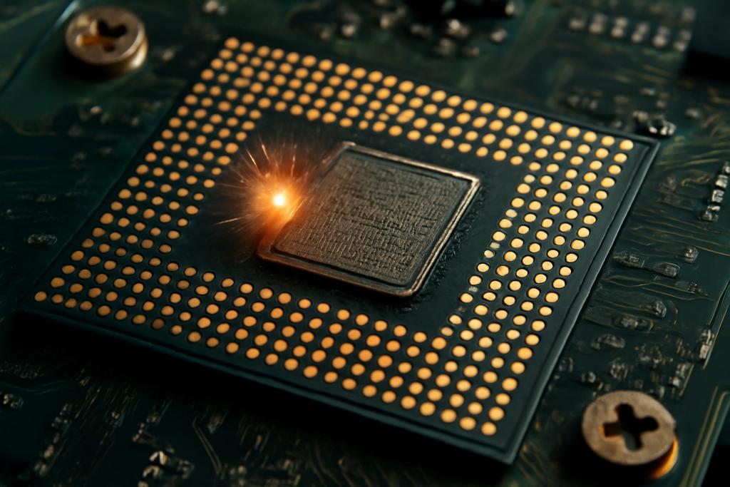
In the quiet, invisible heat of a silicon chip, a tiny spark can ripple into a data flip. Alpha particles—those specks that can ride along from packaging materials into a microprocessor—carry energy that can briefly rearrange the charges inside a memory cell. When that happens in a static random-access memory (SRAM), a stored bit can flip from 0 to 1 or back again. It’s a phenomenon engineers call a single-event upset, and while it sounds like a sci‑fi villain, it’s a real constraint on reliability for devices that need to remember correctly even when the world outside is noisy or hostile. As chips shrink and packing density climbs, the chance that a stray alpha particle will make a memory error grows along with the payoff—speed, energy efficiency, cost—of every transistor you cram into a square millimeter.
Enter a team led by Albert Lu at San Jose State University, with collaborators from Sandia National Laboratories and fellow SJSU researchers. They didn’t just measure alpha-induced glitches; they asked a deeper design question: could we build SRAM in a way that makes it inherently resistant to alpha strikes? Using a combination of first‑principles physics and advanced computer simulations, they proposed a pathway grounded in the architecture of the transistor itself. The core idea is to pair a nanosheet gate-all-around FET—one of the most aggressively scaled transistor geometries—with a bottom dielectric isolation layer that acts like a moat around the chip’s sensitive regions. The result, in their words, is a six-transistor SRAM that could be immune to alpha-particle–induced soft errors, at least in the simulated world. The study’s authors are Albert Lu, Hiu Yung Wong, and Reza Arghavani, and their work sits at the intersection of materials science, electrical engineering, and the kind of design thinking that makes future gadgets more robust without begging for more silicon.
A memory architecture built to stand its ground
The technology behind their idea is not a single gadget but a family of devices designed to push the gate’s influence over the channel to the extreme. Gate-all-around transistors wrap the gate around the channel from all sides, offering tighter control of the flow of electrons than older planar transistors. When you stack three nanosheets to form the channel, you get a nanosheet GAA-FET: a geometry that could help pack more performance into a smaller footprint while reigning in leakage. The study uses two flavors of this device. Type 1 has bottom dielectric isolation (BDI), a dielectric layer tucked under the source/drain region to electrically isolate the channel from the substrate. Type 2 leaves the substrate more directly connected to the nanosheet channel—no BDI in that layout. Both are designed to reflect the sub-7-nanometer design rules that researchers have been chasing as scaling tightens its grip on every transistor’s behavior.
In their integrated SRAM, the architecture remains the familiar 6T cell: two pull-down transistors to hold the data, two pull-up transistors for readout, and two access transistors to gate in a write or read. What changes is where and how the energy from a particle strike can couple into the circuitry. The authors take pains to simulate not just a single transistor but the entire SRAM layout, because the way a strike travels—and which transistors it traverses—depends on the exact arrangement of the devices. Normal operation, the butterfly curves that describe the relationship between node voltages and currents, and the static-noise margins (SNMs) of the two SRAM variants come out similar. The real difference shows up under radiation: the BDI layout restrains how the energy moves and how the circuit can latch onto a fault. In other words, the layout matters as much as the transistor itself.
From the outside, the two SRAM variants look nearly identical in their day-to-day behavior. The genuine distinction is a hidden feature—BDI’s shielding effect on the substrate—which the researchers reveal through careful, damage-path–level simulations. This is where the study slides from a feat of transistor engineering into a design philosophy: you don’t just build a more careful fuse box; you redesign the entire memory so that a stray radioactive particle cannot create a feedback loop that flips a bit.
How alpha strikes travel and what lets memory collapse
To understand why the researchers’ approach could work, you have to understand LET—the linear energy transfer. In simple terms, LET measures how much energy a passing particle deposits per unit length of material as it burrows through the silicon. Alpha particles carry a lot of energy in a tiny track, so they’re particularly good at creating electron‑hole pairs that momentarily perturb the circuit. The team begins by confirming, with ab initio calculations in the PHITS code, that there is a maximum LET for alpha particles in silicon and in silicon-germanium alloys. That maximum turns out to be around 1.54 MeV·cm^2/mg, corresponding to a deposited charge of about 0.0144 picoCoulombs per micrometer in silicon. This LETmax isn’t a universal ceiling for all devices, but it gives a practical benchmark for designing SRAM that can shrug off the worst-case alpha punch.
Once LETmax is in hand, the researchers turn to 3D TCAD simulations to test how the SRAM would respond to strikes at the most vulnerable spots. Their findings hinge on a key idea: a glitch isn’t just the momentary voltage spike at one node. It’s the cascade that can follow when a transient event creates a positive feedback loop across the cell’s cross-coupled inverters. With BDI, that loop is broken more easily, because energy entering the substrate or leaking into the path between source and drain finds fewer channels to exploit. The paper paints a stark contrast: the Type 2 SRAM without BDI flips at relatively modest LET values in several worst-case strike scenarios, whereas the Type 1 SRAM with BDI stays robust even when the simulated LET climbs well past the theoretical LETmax for alpha particles.
In one set of striking examples, they simulate a “channel strike” that traverses through both an off-state access transistor and a pull-down transistor as a hold state ripples through the cell. In this scenario, the Type 2 layout flips at LETmax, while the Type 1 design remains stable even beyond several multiples of LETmax. In a second scenario, a “substrate strike,” where the energy path runs beneath the nanosheets, the Type 2 design flips at a very low LET (0.35 LETmax) but the Type 1 device experiences no flip even at 69 LETmax because the strike’s path doesn’t intersect a sensitive region. In a final test, a “top strike” through three nanosheets near the drain epitaxy produces flips for the Type 2 cell at a low LET, yet Type 1 remains nonresponsive up to high LET values. Across these worst-case strikes, the bottom-die-isolated SRAM consistently proves far more resistant to alpha-induced upset.
The upshot is not merely that BDI helps; it reframes what “radiation hardness” means in a nanoscale SRAM. It isn’t about pushing every transistor to be individually perfect under radiation; it’s about shaping the geometry so that vulnerable regions don’t align in a way that enables a parasitic feedback. It’s a vivid reminder that at the smallest scales, layout—the very arrangement of components on a chip—can be as decisive as the materials or the device structure itself.
The implications: from labs to spacecraft and beyond
What makes this study feel less like a niche engineering curiosity and more like a potential tipping point is where it sits in the broader context of reliability in an increasingly dense, diverse, and radiation-aware technological landscape. First, the work is anchored in solid physics and state-of-the-art simulation. The authors combine ab initio LET calculations with 3D TCAD modeling to bridge the gap between fundamental radiation interactions and practical circuit behavior. That bridge is exactly what industry needs as design rules continue to converge with physics-based reliability concerns. The paper even foregrounds the notion that device-level changes—like inserting a bottom dielectric layer under the source/drain—can dramatically alter how a circuit as a whole responds to a radiation event. It’s a reminder that the path to resilience often travels through clever, well‑reasoned design choices, not just taller walls of shielding materials.
Second, the institutions behind this work matter. The study is a collaboration between San Jose State University and Sandia National Laboratories, with the authorship led by Albert Lu and Hiu Yung Wong of SJSU along with Reza Arghavani of Sandia. The collaboration signals how more and more defense-oriented and high-stakes research is blending university ingenuity with national-lab scale computational power. The result is not a complete shield yet but a concrete design direction that engineers could adopt in future manufacturing flows, especially as we push transistors into sub‑7 nm territory where the geometry itself becomes a tool for reliability, not just a constraint to overcome.
And the scope of potential impact is worth pausing over. In space, where cosmic rays and solar particles bathe electronics, radiation-hardened memory is a constant concern. In nuclear facilities, hospitals with radiation-producing devices, or even autonomous sensors in harsh environments, the ability to prevent memory corruption could translate into fewer soft errors, longer uptime, and lower error-correction overhead. The study’s emphasis on the interplay between transistor physics and layout means that hardware designers could future-proof memory with smarter structures rather than simply adding more error correcting codes or shielding. It’s a shift from “protect the box” to “design the box so that the bug can’t take hold.”
Of course, there are important caveats. what Lu, Wong, Arghavani and their colleagues have shown are simulations guided by ab initio calculations. Real devices, with all the variability of fabrication, packaging, and actual radiation spectra, will still pose challenges. The work is a proof of concept, an invitation to build and test, not a final recipe ready for factory floors. Yet as a proof of concept, it’s beautifully clear: if you can control the vulnerable regions and the feedback paths in a memory cell, you can make a 6T SRAM more resilient to the most insidious kind of “soft” failure. It’s not about eliminating alpha particles; it’s about making memory robust enough that a particle strike becomes a non-event in practice, not just in theory.
Beyond the immediate engineering payoff, the study nudges the field toward a mindset where reliability isn’t a separate layer slapped on after design. It’s an intrinsic property of the device—from the materials chosen to the binding between channel and substrate, all the way to the macro-scale arrangement of transistors. The authors’ use of 3D TCAD simulations to test worst-case strike locations is a blueprint for how future research could quantify robustness across many layout families before a single wafer is manufactured. If these ideas scale, the chips in our satellites, cars, wearables, and data centers might carry a memory that refuses to be swayed by one stray alpha particle, decade after decade.
In the end, the paper offers a provocative takeaway: a memory chip’s future reliability could hinge as much on how its components are laid out as on the charges they store. The team’s message is not that we’ve found a universal shield, but that we’ve identified a design lever—bottom dielectric isolation in nanosheet GAA-FETs—that can drastically raise the bar for radiation hardness. If validated in experiments, this approach could tilt the evolution of SRAM toward architectures where resilience is baked into the architecture, not appended as a postscript. That would be a quiet revolution in how we think about computing hardware for the harsh environments where reliability matters most.