Forget messy chemical baths and painstaking micrometer-scale manipulations. Researchers at Pohang University of Science and Technology (POSTECH), led by Cheol-Joo Kim, have developed a remarkably simple, all-dry method for transferring large-scale graphene films – a feat that could reshape the landscape of electronics and materials science.
The Delicate Dance of Van der Waals Forces
Graphene, a single layer of carbon atoms arranged in a honeycomb lattice, is a wonder material with exceptional electrical conductivity, strength, and flexibility. But harnessing its potential requires a delicate touch. The challenge has always been how to move these incredibly thin sheets from their growth substrate (where they’re initially created) onto other materials without damaging them or introducing impurities that hinder their performance. Previous methods, often involving wet chemical etching processes, introduced contaminants that hampered graphene’s pristine electronic properties.
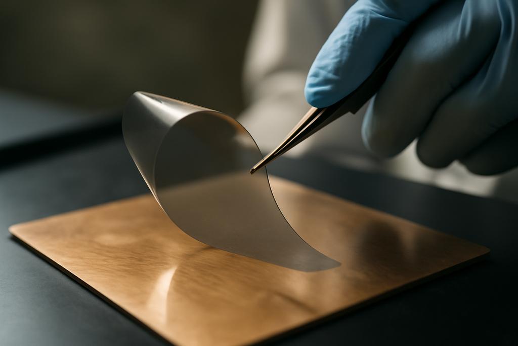
POSTECH’s breakthrough lies in exploiting the subtle yet powerful forces of van der Waals interactions. These weak, attractive forces between molecules (similar to how geckos’ feet stick to walls) are the key to gently lifting and repositioning the graphene film. By cleverly choosing the right materials — growing graphene on a germanium (Ge) substrate and using hexagonal boron nitride (h-BN) as a carrier — the researchers created an environment where van der Waals forces could dominate the transfer process.
Think of it like peeling a sticker from a surface. If the adhesive is too strong, you risk tearing the sticker. But if the adhesive is just right, the sticker comes off cleanly. The POSTECH team has found the ‘just right’ conditions for graphene, creating an ideal balance where the graphene adheres weakly to the germanium and strongly to the h-BN carrier.
Why Ge(110) and h-BN? A Match Made in Materials Heaven
The choice of germanium(110) as the growth substrate is crucial. It presents a surface with a dissimilar lattice structure to graphene, minimizing strong chemical bonds that would resist the delicate pull of the van der Waals forces. The researchers found the adhesion energy between graphene and Ge(110) to be exceptionally low, even lower than the van der Waals interactions between graphene and other layered materials like h-BN.
The h-BN acts as a sturdy, protective carrier. h-BN itself is a layered material, known for its electrical insulation and its ability to preserve the properties of graphene. Using this pairing, the graphene essentially hitches a ride on the h-BN carrier, lifted effortlessly by van der Waals forces. This combination ensures a clean, high-yield transfer process.
A Scalable Solution: From Micrometers to Centimeters
A significant advantage of this technique is its scalability. Previous attempts to transfer graphene using van der Waals forces were largely limited to microscopic samples. POSTECH’s method, however, successfully transfers centimeter-sized graphene films — a huge leap forward for practical applications.
The researchers used a variety of techniques, including optical microscopy, atomic force microscopy (AFM), Raman spectroscopy, transmission electron microscopy (TEM), and X-ray photoelectron spectroscopy (XPS), to confirm the quality and uniformity of the transferred graphene films. The transferred films were exceptionally flat, free from wrinkles and cracks, with extremely low density of atomic defects and minimal charge puddles (small regions of varying charge density that can affect the uniformity of electronic properties). This demonstrates the gentle nature of the transfer process.
Beyond the Transfer: A New Era of Material Assembly
The POSTECH team’s work extends beyond a mere improvement in graphene transfer. It opens up a whole new way to assemble complex materials. The researchers coined a phrase to describe this: the “contact and peel” approach. It works like this: any material of interest can be placed on top of the graphene grown on germanium. Then, just like peeling a sticker, the entire combined structure can be transferred to another substrate, creating various heterostructures with atomically clean interfaces.
This paves the way for the creation of a vast array of new materials with tailored properties. Imagine constructing 3D structures, layer by layer, from different 2D materials. This ‘Lego-like’ assembly could lead to the development of advanced electronic devices, sensors, and other technologies beyond our current imagination.
The Impact: A New Landscape for Electronics
This revolutionary technique could significantly impact the electronics industry. High-quality, large-scale graphene films are essential for the development of faster, more efficient, and flexible electronics. POSTECH’s all-dry transfer method could help unlock graphene’s full potential, leading to innovations in high-speed transistors, flexible displays, and wearable electronics.
The implications extend far beyond electronics. This technique could also revolutionize other fields where the precise assembly of materials is crucial, such as photonics, energy storage, and catalysis. By offering a clean, scalable, and versatile method, POSTECH’s discovery promises a future brimming with exciting possibilities in materials science.