Light loves a good conspiracy. In some engineered materials, its energy glides slowly and stubbornly, as if trapped in a stubborn pocket of space. In others, it roams freely, bouncing from one corner of a structure to another. A photonic flatband is the former: a landscape where the usual rule of thumb, that light velocity changes with direction, seems to dissolve. In this flatland, the group velocity — the speed at which light can carry information or energy — drops to near zero. The effect isn’t boring physics for its own sake; it compounds light–matter interactions, boosts local fields, and can sharpen the response of devices that rely on tiny jolts of light energy.
At the University of Washington, a team led by Minho Choi and Christopher Munley, with Arnab Manna, Arthur Barnard, and Arka Majumdar, has engineered a genuinely two‑dimensional photonic flatband on a silicon metasurface. The geometry is a Lieb lattice, a tidy arrangement that supports a flatband in principle. The remarkable trick here is twofold: they made the flatband robust not just for one polarization or one direction, but across all polarizations and across a meaningful swath of incident angles in two dimensions. In other words, light can linger in place regardless of how you shine it on the surface. This is a rare, practical breath of resilience in a field where flatbands have often been fragile experiments rather than everyday components.
The study, which combines careful fabrication with high‑precision measurement, demonstrates a dispersionsless band across the Brillouin zone near the Γ point for both TE and TM polarizations and for a wide range of angles up to about 60 degrees in some cases. The metasurface is all‑dielectric, built from a crystalline silicon film on sapphire, and tuned with a partial etch and carefully shaped (elliptical) holes to break symmetry just enough to keep the band flat. The result is a high‑quality factor around 300 at near‑visible wavelengths, and a dispersion picture that matches well between rigorous simulations and experiment. This isn’t just a neat optical trick; it opens pathways for compact, robust devices in photodetection, sensing, and even augmented reality where the geometry of light matters as much as its color.
As with many breakthroughs in photonics, the real story isn’t only the end state but the maneuvering required to get there. The team navigated challenges in fabrication, confirmed the physics with Fourier imaging, and showed how a lattice can be nudged to produce a consistent, two‑dimensional flatband that holds up under real‑world lighting. That blend of design intuition, precision engineering, and thoughtful characterization is what makes this more than a clever demonstration. It points to a future where optical components can be created with flat energy landscapes that forgive misalignment and variability, much like how fiber optics replaced bulk optics by weaving resilience into the glass itself.
The Slow World of Flatbands
Flatbands are the optical equivalent of a traffic jam with the lights stuck on red. In a typical photonic crystal, photons travel with a certain speed that depends on their direction and polarization. In a flatband, the energy is available but the group velocity collapses. The energy sits in localized modes, and the density of optical states balloons—more photons are effectively available at a given energy. That combination can dramatically boost nonlinear interactions, meaning the medium responds more strongly to the light, potentially lowering the power you need to drive a response or triggering new phenomena such as nonlinear switching or enhanced sensing.
Historically, the interest in flatbands has been as much about the physics as the potential. In lattices that support flatbands, you can imagine exotic behaviors like quantum scars or the confinement of light in particular regions of a structure purely due to interference. Yet for practical devices, a flatband that only appears in one dimension or under a precise polarization is of limited use. Devices in the wild encounter light from every direction and with every polarization—stray light from a display, ambient illumination, or the diverse angles of real imaging. The dream is a flatband that remains flat no matter how you illuminate it, a sort of isotropic, polarization‑agnostic stage for light–matter interaction.
That broader dream has been slow to materialize, especially in dielectric (non‑metallic) metasurfaces, which promise lower loss and narrower, more controllable resonances than their plasmonic cousins. The ground was laid by previous demonstrations of 1D flatbands or angle‑specific flatbands, but a two‑dimensional flatband that holds for arbitrary two‑dimensional incident angles across polarizations remained elusive. The Washington team didn’t just push the boundary a little; they built a geometry that makes the flatness robust in two dimensions, at least within a meaningful portion of the optical spectrum. The question now is not just whether this flatband exists but how it behaves under the real, messy variety of optical inputs. And the answer, already in their measurements, is a cautiously optimistic yes.
A Two‑Dimensional Flatland Born from a Lieb Lattice
The Lieb lattice is a cousin of the square lattice that, in its idealized form, houses a flatband in a pretty predictable place. It’s a lattice with three sites per unit cell: a central hub and two satellite sites, arranged so that light can interfere in such a way that a band of states becomes perfectly flat. The mathematics of that arrangement is elegant, but turning it into a working optical device requires clever engineering: the lattice must be implemented in a real material, with finite thickness, and its optical modes have to survive the inevitable imperfections of fabrication.
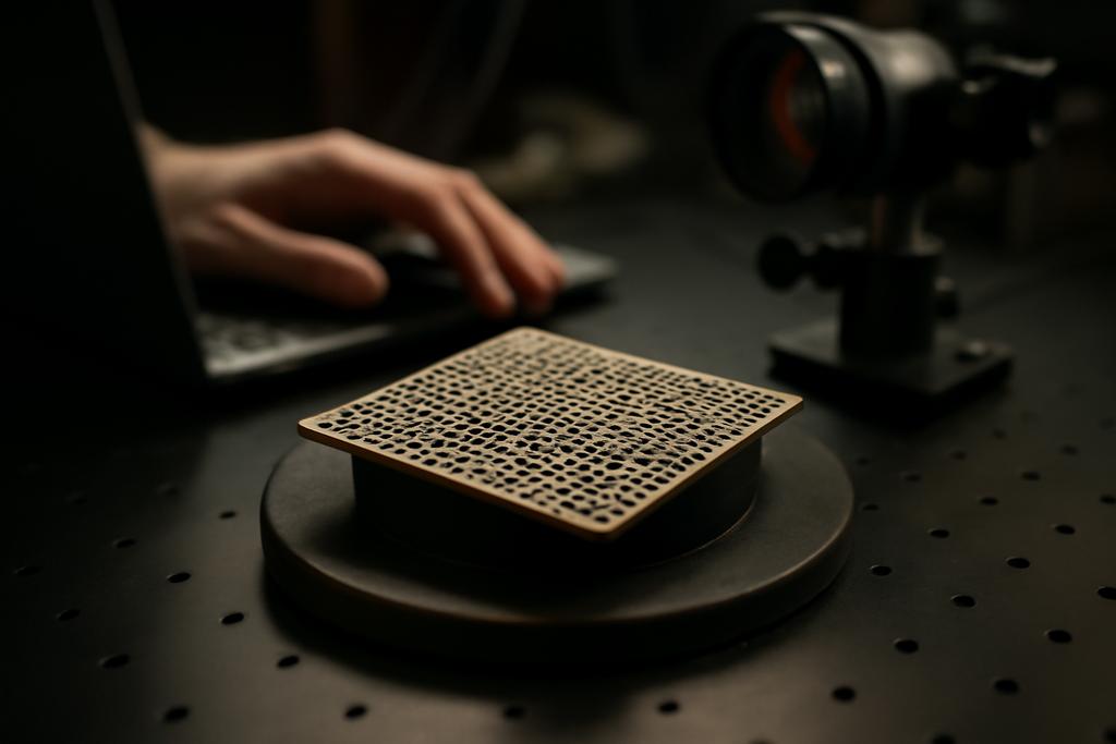
In this work the authors chose a silicon metasurface patterned with a Lieb lattice, designed to break vertical symmetry just enough to help the flatband survive and to extend across multiple directions. They don’t rely on metals; instead they sculpt a dielectric landscape where light travels slowly not because it’s trapped in a metal cavity but because the path it can take is constrained by geometry and interference. The unit cell is small: lattice period around 309 nanometers, with a mix of elliptical and circular voids in a crystalline silicon film baked onto a sapphire substrate. The geometry is tuned so that, near the Γ point of the Brillouin zone, the band becomes locally flat for several polarization states and several crystal directions. The lattice’s symmetry and the way they selectively resize and reshape the holes is what keeps the band from curving into a more familiar, dispersive shape.
One of the sample’s trickier aspects is how they handle the major and minor sublattices. By sculpting the major sublattice elements into ellipses, the team can tune the curvature of the band in different directions and for different polarizations. The result is a band that stays flat across the X–Γ–X and M directions for both S and P polarizations, at least within a meaningful angular range. In physics terms, the degeneracy at the Γ point and the selective confinement to different sublattice elements cooperate to produce a robust flatband that is not tied to a single polarization or a single angle. It’s a careful dance of symmetry breaking and parameter tuning, and the payoff is a genuine two‑dimensional flatland rather than a one‑dimensional curiosity.
All‑Dielectric Engineering, Symmetry Breaking, and Polarization Freedom
To translate the flatband idea into a real device, the team had to fight a familiar foe in photonics: fabrication imperfections. Their approach to tilt this battle in favor of robustness was to work in all‑dielectric material and to exploit a vertical symmetry breaking together with lateral reshaping. The device is a 230‑nm thick crystalline silicon film on sapphire, with a partial etch that delves to about 223 nm in the vertical direction. That partial etch depth is not just a manufacturing detail; it’s a dial that shifts how light couples into and out of the guided resonances. Too little etch and the band curves; too much etch and you risk losing the flatness altogether. The researchers show that with careful calibration and a bit of compensatory redesign of the lateral geometry, the flatband persists even when the depth isn’t perfect.
The practical effect of this geometry is that a single metasurface can behave as a near‑isotropic filter or sensor across a swath of angles and polarizations. The team demonstrates this with a meticulous measurement technique: Fourier imaging combined with energy–momentum spectroscopy. By rotating the sample and rotating the measurement axis, they map the energy of the band as a function of the in‑plane wavevector for many directions. A polarizer before the spectrometer lets them separate S and P polarizations and verify that the flatband holds for both, at least within a central region of the Brillouin zone.
On the simulation side, the team uses rigorous coupled wave analysis to predict the band structure and then compares it to the experiment. The agreement is strikingly close, with a small wavelength offset of about 10 nanometers between theory and measurement. That offset, the authors note, likely stems from a modestly overetched depth in the actual device, which their data and additional modeling suggest can be compensated by tweaking the lateral geometry. It’s a reminder that in nanostructured optics, the devil is in the details, but the design language still tends to win out when you’re chasing a robust physical principle rather than a single, perfect specimen.
So what does a dispersionless two‑dimensional band actually enable in practice? The immediate answer is not a magic laser but a more reliable stage for light–matter interactions. A flatband concentrates optical energy in space and time, elevating local field strengths and density of states. That, in turn, can amplify nonlinear effects, improve the efficiency of light harvesting, and increase sensitivity in detectors. For devices that rely on precise angle or polarization responses—think compact filters, sensors, or imaging optics—having a flatband that ignores most of those variables can dramatically reduce alignment headaches and size penalties.
The Washington team highlights several potential applications. Local field enhancement is one, where strong, confined light can boost nonlinear processes or encourage more efficient absorption in ultra‑thin detectors. They also point to augmented reality as a practical arena. An all‑dielectric flatband metasurface could act as a compact, high‑Q optical element that remains stable as a user tilts their head or moves the device, potentially enabling more robust eye‑tracking, better color filtering, or more compact, integrated sensor suites in AR displays. In the long run, such flatbands could underpin narrowband light sources or sensors that don’t care about the exact angle of incidence—a kind of optical “grace under pressure.”
And there’s a deeper resonance, too. Flatbands have always offered a playground for exploring exotic physics in controlled settings. A truly two‑dimensional, polarization‑agnostic flatband on a dielectric platform nudges that playground closer to practical devices. It’s the kind of result that says geometry—how you arrange tiny voids, how you break symmetry just enough, how you channel energy through a lattice—can do as much work as material choice or complex fabrication chains. The architecture invites a broader design philosophy: instead of chasing perfect, angle‑specific resonances, build flat energy landscapes that tolerate the real world’s imperfections and still sing when light enters from unexpected directions.
A Roadmap, Not a Finished Road
There are caveats worth keeping in mind. The demonstrated flatband spans a numerical aperture around 0.1 for true polarization‑independent behavior, with some polarizations extending up to 0.4 for select directions. That’s a strong result, but it also marks a practical boundary: the current design achieves dispersionless behavior over a meaningful, yet finite, region of angle and polarization. Extending this to even larger angular acceptance or to broader spectral ranges will require further refinement—likely more nuanced control of the etch process, sublattice geometry, and perhaps integrating different dielectrics or multi‑layer stacks to tailor losses and coupling.
Another path worth watching is the potential role of circular polarization in decoupling incident angle from the band’s orientation. The authors hint at this as a promising route. If circularly polarized illumination could unlock flatness across even more angular ranges, we’d be looking at a truly robust, multi‑polarization platform for optical components that stay steady as we move around them or as light comes from unpredictable angles. Such advances would be particularly welcome in wearable tech, head‑mounted displays, and portable sensing where rigid alignment is simply not feasible.
From a fabrication standpoint, achieving consistent flatbands across many devices will demand tight control over the geometry. The study’s approach—tuning partial etch depth and adjusting lateral parameters for each device to recover flatness—shows the path forward but also signals that manufacturing at scale will need systematic process controls and perhaps design rules that are robust to typical manufacturing tolerances. The science is compelling; the engineering challenge now is translating that into repeatable, scalable production lines that can produce many devices with the same flatband temperament.
A New Chapter for Optical Design
What we’re watching is a shift in the way people think about optical components. Rather than chasing a single spectral feature with a razor‑thin tolerance, researchers are building landscapes in which light happily lingers and responds in a controlled, predictable way no matter which direction it comes from. The two‑dimensional flatband on a Lieb lattice, realized in a silicon metasurface, is a vivid example of this philosophy in action. It combines a deep understanding of lattice physics with the practicalities of modern nanofabrication to deliver something that feels both fundamental and deployable.
As the field moves forward, the clues suggest that we’ll see more dielectric metasurfaces that exploit flatbands not as curiosities but as underlying design primitives. Imagine compact spectrometers and filters that don’t require fine alignment, or highly efficient, angle‑tolerant photodetectors integrated directly onto chips. Or AR components that filter, steer, and detect light with minimal fuss about how the user is looking at the device. The core idea—making light slow, localizing it in two dimensions, and making that localization robust to the way we illuminate it—could become a staple design principle in the next generation of photonic systems.
In the words of the researchers behind this work, the draft of what a truly versatile two‑dimensional flatband can do is just being written. Their combination of experimental finesse, rigorous modeling, and a practical eye for real‑world use makes it more plausible than ever that these ideas will migrate from the lab bench to everyday technology. The University of Washington team’s achievement is not a final answer but a compelling invitation to reimagine how we weave light through matter, one carefully shaped lattice at a time.
Lead authors and institutions Minho Choi, Christopher Munley, Arnab Manna, Arthur Barnard, and Arka Majumdar led the study at the University of Washington in Seattle, with contributing work from the Laboratory for Physical Sciences. This collaboration blends electrical engineering, physics, and nanofabrication to push the boundaries of how light can be controlled by design.