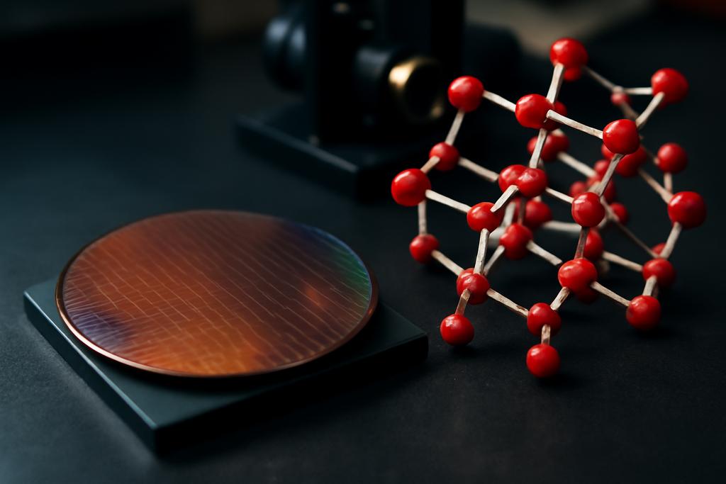
When Silicon Hits Its Limits, Molecules Step In
Silicon photonics has been the backbone of modern optical communication, enabling data to zip through fiber networks at blistering speeds. But silicon itself has a stubborn blind spot: it doesn’t exhibit the electro-optic (EO) effect known as the Pockels effect, which is crucial for ultrafast, energy-efficient modulation of light signals on a chip. This limitation has pushed researchers to look beyond silicon, hunting for materials that can be integrated with silicon to create hybrid devices that combine the best of both worlds.
Enter the world of electro-optic molecular crystals, a class of materials that have been largely overlooked for integrated photonics due to their tricky film formation. Yet, a team at Japan’s National Institute of Advanced Industrial Science and Technology (AIST), led by Keishi Sunami and Jun’ya Tsutsumi, has flipped this narrative by discovering molecular crystals that not only pack a punch in EO performance but also play nicely with silicon fabrication processes and withstand the heat of real-world devices.
Why Electro-Optic Materials Matter
Optical modulators are the gatekeepers converting electrical signals into optical ones on silicon chips. Traditional silicon modulators rely on the plasma dispersion effect, which is hitting a performance ceiling. EO modulators, which leverage the Pockels effect, promise faster speeds and lower power consumption. But silicon’s lack of this effect means we need to graft EO-active materials onto silicon waveguides.
Materials like lithium niobate have been the go-to EO materials, prized for their stability and low optical loss. However, integrating lithium niobate onto silicon is a delicate dance involving bonding and alignment that complicates manufacturing. EO polymers offer a more flexible alternative with higher EO activity and easier deposition, but they suffer from thermal instability — their molecular alignment relaxes over time, especially under heat, degrading performance.
Cracking the Code of Molecular Crystals
Molecular crystals, such as 4-(4’-nitrophenylazo)diphenylamine (NDPA) and its cousin PNPA, have long been known for their nonlinear optical properties. Unlike polymers, their molecules naturally align in the crystal lattice, sidestepping the need for electric-field poling and the associated thermal instability. The catch? Their crystal growth tends to be anisotropic and unpredictable, making it hard to form uniform thin films essential for integrated photonics.
The AIST team tackled this head-on by developing a clever materials screening strategy that goes beyond just looking at molecular hyperpolarizability (a measure of EO potential). They introduced a crystal habit parameter, I2D, which predicts how a crystal grows — whether in one, two, or three dimensions — and combined this with melting point data to assess thermal stability and processability.
This approach led them to identify NDPA and PNPA as molecular crystals with the sweet spot of high EO activity, two-dimensional crystal growth (which favors thin-film formation), and melting points conducive to melt casting — a process where the material is melted and allowed to solidify into a thin film.
Melt Casting Meets Silicon Slots
Using melt casting, the researchers demonstrated that NDPA and PNPA could form large, high-quality single-crystal films over 1000 micrometers in size. Even more impressively, these films could be grown inside ultra-narrow silicon slots as small as 140 nanometers wide — the scale used in slot waveguide modulators — by capillary action. This compatibility with silicon nanostructures is a game-changer for integrating EO materials directly onto silicon photonic chips.
Electro-Optic Performance That Turns Heads
Measuring EO activity is no trivial task, but the team employed a sophisticated birefringence ferroelectric field-modulation imaging technique to quantify the EO coefficients of these films. The results? NDPA and PNPA exhibited EO coefficients (n33r33) exceeding 700 pm/V, more than double that of lithium niobate and on par with the best EO polymers.
What sets these molecular crystals apart is their thermal resilience. The EO performance remained stable even after 1000 hours at 393 K (about 120 °C), a temperature at which EO polymers typically degrade significantly. When sealed to prevent sublimation, the films showed virtually no loss in EO activity, underscoring their robustness for real-world device operation.
Aligning Crystals Without Electric Fields
One hurdle for EO materials is controlling the orientation of their crystal polar axis to maximize EO efficiency. Polymers require electric-field poling, a complex step that can limit scalability. The AIST team discovered that by applying a temperature gradient during melt casting, they could coax the crystals to grow with a preferred orientation over millimeter-scale domains — large enough for practical device lengths.
This temperature-gradient method offers a scalable, elegant alternative to poling, potentially simplifying manufacturing and improving device uniformity.
Designing the Future of Photonics
The success of NDPA and PNPA stems from a thoughtful molecular design: strong electron donor and acceptor groups connected by extended π-conjugated bonds, which boost hyperpolarizability and thermal stability. Coupled with the crystal habit prediction focusing on two-dimensional growth, this strategy opens a new pathway to discover and engineer EO molecular crystals tailored for silicon photonics.
Why This Matters
The findings from AIST challenge the long-held assumption that molecular crystals are unsuitable for integrated photonics due to poor film formation. By demonstrating high EO performance, excellent thermal stability, and compatibility with silicon nanostructures, these materials could leapfrog current EO polymers and lithium niobate in next-generation optical modulators.
As data traffic surges and AI demands ever-faster communication, the ability to integrate robust, high-performance EO materials directly onto silicon chips is critical. Molecular crystals like NDPA and PNPA might just be the dark horses that rewrite the rules of photonic integration, enabling faster, smaller, and more energy-efficient optical devices.
Keishi Sunami, Sachio Horiuchi, Yoriko Sonoda, Naomi Fujiki, Toshiki Higashino, Yuki Atsumi, Shoji Ishibashi, and Jun’ya Tsutsumi from the National Institute of Advanced Industrial Science and Technology (AIST) in Tsukuba, Japan, spearheaded this breakthrough, blending chemistry, materials science, and photonics into a compelling vision for the future.


