Revolutionizing the Design of Optoelectronic Devices
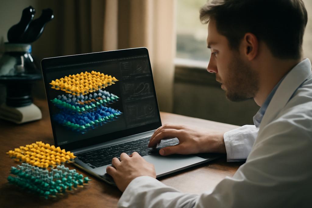
The world of electronics is on the brink of a revolution. We’re not just talking incremental improvements, but a fundamental shift in how we design and build the devices that power our lives. At the heart of this transformation lies the fascinating realm of two-dimensional (2D) materials, ultrathin substances with properties that defy conventional expectations. Imagine stacking these atomically precise sheets like building blocks, creating entirely new materials with bespoke functionalities – that’s the promise of 2D material heterostructures.
But there’s a catch. Predicting the behavior of these heterostructures – how they’ll respond to light, conduct electricity, and interact with other components – requires incredibly complex calculations. Traditional methods are often computationally prohibitive, especially when dealing with the large unit cells characteristic of these complex structures. This is where the exciting research by Maximilian Schebek, Ignacio Gonzalez Oliva, and Claudia Draxl of Humboldt-Universit¨at zu Berlin comes in.
A Smarter Approach to Complex Calculations
Schebek, Gonzalez Oliva, and Draxl’s breakthrough centers around a clever computational strategy. Instead of tackling the entire heterostructure as a single, overwhelmingly complex entity, they’ve devised a method that cleverly breaks down the problem into smaller, more manageable pieces. Think of it like assembling a complex Lego castle: instead of trying to build every brick simultaneously, they calculate the properties of individual components and then add them together, taking advantage of the fact that many 2D heterostructures are held together by weak van der Waals forces.
This “expansion & addition screening” (EAS) method isn’t just a slight tweak; it’s a fundamental reimagining of the computational approach. The researchers extend their previous work, which used planewave basis sets, to encompass the more sophisticated (linearized) augmented planewave (L)APW method, which offers a more precise, all-electron description of the material’s electronic structure. This is a significant advancement, as it allows for a higher level of accuracy and deeper understanding of the heterostructure’s properties.
Beyond the Bilayer: Implications for Hybrid Materials
To showcase the power of their method, the researchers applied their EAS approach to two prototypical systems: a tungsten diselenide (WSe2) bilayer and a hybrid inorganic-organic system (HIOS) consisting of pyridine molecules adsorbed on a molybdenum disulfide (MoS2) monolayer. The results were striking. The EAS method accurately predicted the quasi-particle band structures (which describe the energy levels of electrons within the material) and optical absorption spectra (which show how the material interacts with light) of both systems, matching the results obtained through far more computationally intensive conventional methods.
The implications are far-reaching. Designing new optoelectronic devices—like solar cells, LEDs, and sensors—typically requires extensive experimentation and testing. But with the ability to accurately predict the properties of complex heterostructures using vastly reduced computing resources, researchers can accelerate this process dramatically. The EAS method allows exploration of a far greater range of combinations of 2D materials, leading to the discovery of materials with unprecedented properties, tailored to specific applications.
A New Era of Computational Materials Science
The researchers’ work doesn’t simply improve existing computational methods; it fundamentally shifts the boundaries of what’s computationally feasible. Their EAS method dramatically reduces the computational cost associated with the calculations, effectively bringing previously inaccessible simulations within the reach of many research groups. The speed increase isn’t a small improvement—in their tests, the EAS method slashed computation time by over 50% for GW calculations and by almost 70% for Bethe-Salpeter Equation (BSE) calculations, which are used to predict optical properties.
While the complete calculation time isn’t reduced by the same amount—because some steps remain computationally expensive regardless of the screening method—the decrease is significant. This increase in efficiency opens new possibilities for researchers working with all-electron calculations, allowing them to study larger, more complex heterostructures and explore more subtle effects. This kind of advancement isn’t just about faster computers; it’s about expanding our fundamental understanding of materials and paving the way for innovation in diverse technologies.
Looking Ahead: The Future of Heterostructure Design
The development of EAS marks a crucial step forward in computational materials science. By providing a highly efficient method for calculating the properties of complex 2D material heterostructures, Schebek, Gonzalez Oliva, and Draxl have made a substantial contribution to materials discovery and design. This work doesn’t just streamline existing procedures; it unlocks previously inaccessible realms of materials research, enabling scientists to investigate a wider range of novel materials with unprecedented accuracy and efficiency. The future of optoelectronics and beyond may well be built on the foundation of this breakthrough.


